|
|
|
|
|
|
|
|
|
|
|
|
|
|
|
|
|
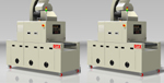
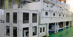
UV 경화 시스템, 모듈형 UV 경화시스템 UV 세정 시스템 UV 노광 시스템 SPOT UV, UV LED FLOOD UV 외 |
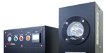
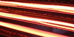
MIR / NIR 건조시스템 적외선 건조시스템 IR / 열풍 건조시스템 소성로 (FIRING FURNACE) |
펄스UV 경화 시스템 펄스UV 세정 시스템 외 |
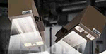
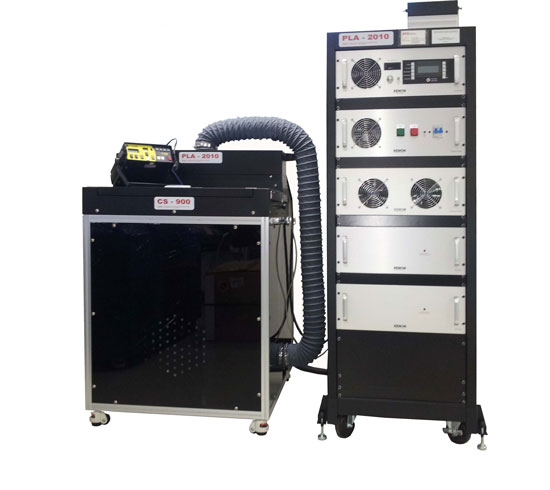
제논 조사장치 75W, 100W, 150W 200W, 300W, 1 kW 3 kW ~ Max. 15 kW
|
내후성 시험장비 WEATHER TESTER 기타 주문형 시험장비 |
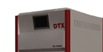
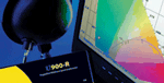
광량계, 광계측기 광분석시스템 광모니터링 시스템 외 |
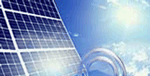
솔라셀 제조장비 SOLAR FIRING SOLAR SIMULATOR (CELL, MODULE) SOLAR CELL PRINTING |
|
|
|
|
|
|
|
|
|
|
|
|
|
|
|
|
|
|
|
|
|
|
|
|
|
|
|
|
|
|
|
|
|
X-UV 경화 시스템 PHOTONIC ACTIVATION X-UV 살균, 세정 외 |
MIR / NIR 램프, 제논램프 펄스UV램프 솔라시뮬레이션 램프 외
|
X-LIGHT 어닐링 시스템 PHOTONIC CURING SYS |
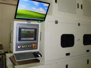
(자동, 반자동, 인라인) |
|
LED BLU 휘도 검사시스템 LED 조도 검사시스템 SWIR검사, X-RAY검사 NEUTRON 검사시스템 |
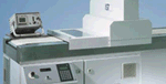
솔라셀 제조 라인 인쇄 코팅, 전처리, 건조, 경화 생산 라인 롤 코터 / DIP 코터 라인
|